- 您现在的位置:买卖IC网 > Sheet目录2009 > MAX3992UTG+T (Maxim Integrated Products)IC DATA RECOVERY W/EQ 24-TQFN
MAX3992
Applications Information
Exposed Pad (EP) Package
The exposed pad, 24-pin QFN incorporates features
that provide a very low thermal-resistance path for heat
removal from the IC. The pad is electrical ground on the
MAX3992 and must be soldered to the circuit board for
proper thermal and electrical performance.
Layout Considerations
For best performance, use good high-frequency layout
techniques. Filter voltage supplies, keep ground con-
nections short, and use multiple vias where possible.
Use controlled-impedance transmission lines to inter-
face with the MAX3992 high-speed inputs and outputs.
Power-supply decoupling should be placed as close to
VCC as possible. To reduce feedthrough, take care to
isolate the input signals from the output signals.
10Gbps Clock and Data Recovery
with Equalizer
10
______________________________________________________________________________________
Table 3. Functional Control
FCTL1
FCTL2
DESCRIPTION
00
Normal operation, serial clock output
disabled.
1
0
Standby power-down mode.
01
Normal operation, serial clock output
disabled.
11
Serial clock output enabled for jitter
testing.
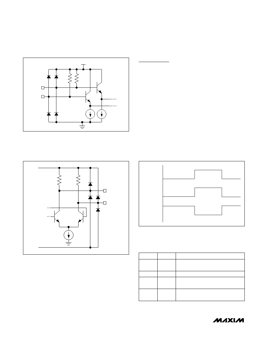
Figure 5. CML Input Model
SDI+
SDI-
VCC
50
Figure 6. CML Output Model
VCC
GND
SDO+
SDO-
50
Figure 7. Polarity (POL) Function
(SDI+) - (SDI-)
(SDO+) - (SDO-)
POL = VCC
(SDO+) - (SDO-)
POL = GND
发布紧急采购,3分钟左右您将得到回复。
相关PDF资料
MAX504EPD+
IC DAC 10BIT 5V LP SER 14-DIP
MAX507AENG+
IC DAC 12BIT W/REF 24-DIP
MAX5100AEUP+T
IC DAC 8BIT QUAD R-R 20TSSOP
MAX5101BEUE+
IC DAC 8BIT TRPL R-R 16-TSSOP
MAX5102AEUE+T
IC DAC 8BIT DUAL PAR-IN 16-TSSOP
MAX5104EEE+T
IC DAC 12BIT DUAL SER 16-QSOP
MAX5106EEE+T
IC DAC 8BIT QUAD NV 16-QSOP
MAX5109EEE+
IC DAC 8BIT DUAL NV 16-QSOP
相关代理商/技术参数
MAX3996CGP
功能描述:激光驱动器 3-5.5V 2.5Gbps VCSEL & Laser Driver RoHS:否 制造商:Micrel 数据速率:4.25 Gbps 工作电源电压:3 V to 3.6 V 电源电流:80 mA 最大工作温度:+ 85 C 封装 / 箱体:QFN-16 封装:Tube
MAX3996CGP-T
功能描述:激光驱动器 3-5.5V 2.5Gbps VCSEL & Laser Driver RoHS:否 制造商:Micrel 数据速率:4.25 Gbps 工作电源电压:3 V to 3.6 V 电源电流:80 mA 最大工作温度:+ 85 C 封装 / 箱体:QFN-16 封装:Tube
MAX3996CTP+
功能描述:激光驱动器 3-5.5V 2.5Gbps VCSEL & Laser Driver RoHS:否 制造商:Micrel 数据速率:4.25 Gbps 工作电源电压:3 V to 3.6 V 电源电流:80 mA 最大工作温度:+ 85 C 封装 / 箱体:QFN-16 封装:Tube
MAX3996CTP+D
制造商:Maxim Integrated Products 功能描述:LASER DRVR VCSEL 2.5GBPS 1CH 20TQFN - Rail/Tube
MAX3996CTP+T
功能描述:激光驱动器 3-5.5V 2.5Gbps VCSEL & Laser Driver RoHS:否 制造商:Micrel 数据速率:4.25 Gbps 工作电源电压:3 V to 3.6 V 电源电流:80 mA 最大工作温度:+ 85 C 封装 / 箱体:QFN-16 封装:Tube
MAX3996CTP+TD
制造商:Maxim Integrated Products 功能描述:LASER DRVR VCSEL 2.5GBPS 1CH 20TQFN - Tape and Reel
MAX3996EVKIT
功能描述:激光驱动器 Evaluation Kit for the MAX3996 RoHS:否 制造商:Micrel 数据速率:4.25 Gbps 工作电源电压:3 V to 3.6 V 电源电流:80 mA 最大工作温度:+ 85 C 封装 / 箱体:QFN-16 封装:Tube
MAX3997ETM+
制造商:Maxim Integrated Products 功能描述:4 CH 10.3G LIMITING AND LINEAR EQ - Rail/Tube